Kamagra gibt es auch als Kautabletten, die sich schneller auflösen als normale Pillen. Manche Patienten empfinden das als angenehmer. Wer sich informieren will, findet Hinweise unter kamagra kautabletten.
Sscas.ee.ncku.edu.tw
JOURNAL OF ELECTRONIC TESTING: Theory and Applications 18, 571–581, 2002
� 2002 Kluwer Academic Publishers. Manufactured in The Netherlands.
Structural Fault Based Specification Reduction for Testing Analog Circuits
SOON-JYH CHANG AND CHUNG LEN LEE
Department of Electronic Engineering & Institute of Electronics, National Chiao Tung University,
Hsin-Chu, Taiwan, Republic of China
Department of Electrical Engineering, Chung-Hua University, Hsin-Chu, Taiwan, Republic of China
Received October 5, 2001; Revised May 8, 2002
Editor: K.J. Antreich
Specification reduction can reduce test time, consequently, test cost. In this paper, a methodology to
reduce specifications during specification testing for analog circuit is proposed and demonstrated. It starts withfirst deriving relationships between specifications and parameter variations of the circuit-under-test (CUT) and thenreduces specifications by considering bounds of parameter variations. A statistical approach by taking into accountof circuit fabrication process fluctuation is also employed and the result shows that the specification reductiondepends on the testing confidence. A continuous-time state-variable benchmark filter circuit is applied with thismethodology to demonstrate the effectiveness of the approach.
analog test, test cost reduction, specification-based test, fault-based test
based testing, it is to measure some specified perfor-mance specifications of the CUT, such as DC gain,
Analog circuit testing has been a difficult problem, pri-
cut-off frequency, and slew rate, etc., and to determine
marily due to the non-deterministic nature of compo-
"pass" or "fail" of the CUT based on whether the mea-
nent parameters and limited accessibility of internal
sured results are within specified ranges. This test ap-
nodes for the CUT. Analog testing techniques are tra-
proach is straightforward and is easy to be applied.
ditionally classified into two categories, i.e., structural
However, it lacks precise metrics to indicate the struc-
(fault)-oriented testing and functional (specification)-
tural fault coverage and is inherently expensive since it
based testing. For the structure-oriented testing, a fault
involves expensive dedicated test equipment and long
model, usually at the circuit level, is adopted and pat-
testing time.
terns (signals) are applied to the CUT to exploit the
Several researches [1, 10, 17] that alleviate the diffi-
specific structural difference between the defective and
culty of test generation, fault classification, test quality
non-defective circuits. However, there are no univer-
improvement for analog and mixed-signal testing have
sally accepted fault models for analog circuits because
been presented by linking the information of structural
the nature of analog faults is not constant and cannot
fault and circuit specifications. One important goal on
be definitely and precisely modeled. For the functional-
testing research is to reduce the test time. In the digital
Chang, Lee and Chen
domain, this corresponds to deriving the efficient test
Mapping Between Faults and Specifications
set which maximizes fault detection. In the analog do-main, due to the difficulty in defining faults as men-
As mentioned previously, there is no universal and
tioned above, there were only a few works on this topic.
well-defined fault model for testing analog circuits.
Huss et al. [4] studied the problem by ordering specifi-
A common practice is to resort to the circuit level to
cation tests so that faulty circuits are detected early in
define a fault to be an "open" or "short" of a circuit
the test sequence to reduce the average test time. This
component such as a resistor, capacitor or a transistor
approach is efficient to reduce test time if a CUT is
etc. (catastrophic faults), or a deviation on the value
defective but does not gain advantage when the circuit
of the above circuit components (parametric faults).
is normal. Milor and Sangiovanni-Vincentelli [9] also
These faults are used because they generally can be
proposed an algorithm for finding an ordering of speci-
clearly attributed from physical manufacturing defects
fication tests to increase the efficiency of the functional
and deduced from the computer-aided analysis such as
testing. This algorithm eliminates the non-critical spec-
Inductive Fault Analysis (IFA) [8, 11, 14, 18]. They are
ifications based on the yield prediction but it is hard
relatively well defined and easier to be handled. They
to derive the accurate yield and it is time-consuming
can be served as a metric for evaluating the testing
when correlations between specifications are consid-
coverage and the effectiveness of tests for testing ana-
ered. Souders and Stenbakken [15] presented an ap-
log circuits. It has been shown [9, 16] that parametric
proach to select a minimal set of basis vector to calcu-
faults are significantly more important to be considered
late the entire behavior for analog-to-digital converter.
since they dominate catastrophic faults and are harder
This method reduces the test time but needs extra inter-
to be detected. In this work, specifications are stud-
nal test points for the CUT. Lindermeir et al. [7] pro-
ied to be reduced while considering parametric faults
posed a characteristic observation inference test design
as the metric. Circuit parameters such as resistances,
approach for analog circuit. For the approach, for each
capacitances, inductances passive components and
VT
given specification, it simulates training samples and
(threshold voltage),
W (channel width) and
L (chan-
computes a test inference criterion based on a logis-
nel length) of the MOS transistors are within their al-
tic discrimination analysis. With obtained test criteria,
lowable range, i.e. within specified fluctuations of the
satisfaction or violation of the original circuit specifi-
manufacturing process. When a parametric fault oc-
cations are inferred from characteristic observations of
curs, possibly caused by a local defect or manufactur-
the circuit under test.
ing equipment error, the value of the circuit parameter
In this paper, we approach this problem by study-
is outside of the range of the specified range.
ing the relationship between the performance specifi-cations with component parameters of the analog CUT
Mapping Specifications to Circuit Parameters
and reaching the conclusion that some of specificationsof the circuit can be removed for the testing purpose.
Consider a circuit of
m parameters,
P = [
p1
, p2
, . . ,
By removing the specification, the testing time can be
pm], where
pi could be resistances of resistor, ca-
reduced. Also, a statistical approach is employed by
pacitance of capacitor,
W/L ratio of transistor, and
taking into account of circuit fabrication process fluc-
VT of transistor, etc. The performance of the circuit
tuation to show that the specification reduction depends
is bounded by
n specifications,
S = [
s1
, s2
, . . , sn].
on the testing confidence.
Su = [
su, su, . . , su] and
Sl = [
sl , sl , . . , sl ] are de-
The paper is organized as follows: The fault model
noted to the upper and lower bounds for these spec-
and the procedure to derive the relationships between
ifications. For the design with the nominal
P value:
analog faults and specifications are first presented with
P0 = [
p0
, p0
, . . , p0 ], we can find a corresponding
a simple low pass filter as an illustration example.
point,
S0 = [
s0
, s0
, . . , s0], in the specification space.
Then, Monte Carlo simulation is used to find the ef-
Fig. 1 shows the abstract graph of mapping between
fect of the manufacturing process fluctuation on the
the parameter space and the specification space. Also,
above relationships, and a specification reduction pro-
it is an aim to conversely find the accepted tolerances of
cedure is described. An illustrative case study on the
parameters from the allowed ranges of specifications.
continuous-time state-variable filter benchmark circuit
Under the single fault assumption, the accepted tol-
[6] is included to demonstrate the effectiveness of the
erance of each parameter can be obtained through de-
duction if the relationship between specifications and
Structural Fault Based Specification Reduction
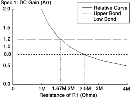
2 (M�). The ranges for each specification are as shownin the figure. By solving 0.8 ≤ s1( p1) = −2 (M�) ≤
1.2, we obtain that the accepted range of p1 for s1 is1.667 (M�) ≤ R1 ≤ 2.5 (M�), i.e., pu = 2.5 (M�)
and pl = 1.667 (M�). The upper and lower bounds of
accepted range of R1 for s2 is pu = ∞ and pl = −∞
since s2( p1) =
is independent of R
Fig. 1.
Mapping between the parameter and the spec-
we can obtain pu = ∞, and pl = 1 (M�) by solving
ification space [10, 17].
s3( p1) = R1 ≥ 1 (M�).
The above deductive approach is efficient if the re-
parameters are explicit and simple or through simula-
lationships between parameters and specifications are
tion combined with back-inference. A simple example
explicit and simple. However, these relationships are
will be used to explain this later.
usually implicit and hard to be derived when circuits
For a specification, say, the j th specification s j ∈
are large and active components are involved. For these
S, it is a function of all parameters p's. If, un-
cases, simulation-based approach needs to be used.
der the single fault condition, we consider parameter
That is: the deviations of specifications w.r.t. param-
pi , s j can be represented as s j ( pi ) = f ( p1, p2, . . ,
eters are directly simulated. The relationships between
pi−1, pi , pi+1, . . , pm) where all pi 's are fixed ex-
specifications and parameters can be obtained in ta-
cept pi which is allowed to vary. We assume that s j
ble or curve forms and bounds of the parameters can
is bounded by su and sl , the accepted process toler-
be found by applying the constraints of specifications
ance range of pi for s j can be deduced by solving the
on these relationships. Fig. 3 shows such a curve of
specification Ao of the low pass filter circuit of Fig. 2
w.r.t. parameter R1. The upper and lower bounds for R1
s j ( pi ) = f p0, p0, . . , p0 , p
, . . , p0 ≤ su
for this specification A
o can be extracted to be 2.5 and
1.67 (M�) respectively. In a similar way, the bounds of
s j ( pi ) = f p0, p0, . . , p0 , p
, . . , p0 ≥ sl
all other parameters w.r.t. the respective specificationscan be derived and are shown in Table 1.
We denote the obtained upper and lower bounds ofaccepted range of pi for s j to be pu and pl respectively.
A simple low pass filter of Fig. 2 is used as the ex-
Procedure of Specification Reduction
ample to explain as follows:
The transfer function of the low pass filter is:
A circuit is defined as "fault-free" if it satisfies all theconstraints of specifications. Thus, the final upper ( pu)
Assume that the parameters we consider are R1, R2,and C and the specifications are DC gain A0, cut-offfrequency fc, input resistance Rin, respectively. For
R1 = 2 (M�), R2 = 2 (M�), and C = 100 (pF), A0 =
−R2 = 1, f
= 795.8 (Hz) and R
in = R1 =
2π R2C
Design parameters:
1 = 2 (MΩ)
R2 = 2 (MΩ) …
C = 100 (pF) …
0.8 ≤ A0 ≤ 1.2
600 (Hz) ≤ fc ≤ 1 (KHz) … s2Rin ≥ 1 (MΩ)
Fig. 2.
A low pass filter example to explain the deduction of rela-
Fig. 3.
Relationship curve of specification Ao w.r.t. parameter R1
tionship between parameters and specifications.
of the example circuit of Fig. 2.
Chang, Lee and Chen
Table 1.
Upper and lower bounds of R1, R2 and C w.r.t. specifi-
Table 2.
Tolerance range and the most significant
cations A0, fc and Rin.
specifications for decreasement and increasementfaults of each parameter.
R1 (�)
R1 (�)
R2 (�)
R2 (�)
C (F)
FLB: final lower bound; FUB: final upper bound.
UB: upper bound. LB: lower bound.
and lower bounds ( pl ) of accepted range for i th param-
Table 2 summarizes the tolerance range of all pa-
rameters and the most significant specifications for
the decreasement and the increasement faults of each
pu = minimum pu , pu , . . , pu
parameter. From the table, apparently, s1 and s2 are
the essential test specifications which need to be con-
pl = maximum pl , pl , . . , pl
sidered in testing as all the parameters: R1, R2, and
For the low pass filter example shown above, the
C are considered, but s3 can be ignored. That is:
final upper and lower bounds of R
specifications are reduced from s1, s2, and s3 to s1
1 should be given
to be minimum(2.5 M�, ∞, ∞) ⇒ 2.5 (M�) and
and s2.
maximum(1.67 M�, −∞, 1 M�) ⇒ 1.67 (M�) re-spectively. Hence, if the resistance deviation, causedby a defect, of R
The Impact of Manufacturing
1 is within the range of 2.5 (M�)
and 1.67 (M�), the circuit will pass all specifica-
tions s1, s2 and s3 and will be considered to begood.
As feature size of MOSVLSI moves into the deep sub-
In the above, s1 is the most significant specification
micron range, the device characteristics and yield be-
in determining the lower bound for the R
come more sensitive to manufacturing process fluctua-
ment fault since it is the specification which determines
tions. When there are variations in the parameter space
the lower bound for R
due to the process fluctuation, correspondingly, there
1. This specification is the "Es-
sential Lower Bound Specification for parameter i",
will be variations on the specification space of the cir-
denoted to be ELBS
cuit. The specification and the parameter relationship
i , which is given by the general
such as that of Fig. 3 will become a band instead of asingle curve due to value variations, which are caused
by the process fluctuation, of all parameters as shown
i = s j pl =pl , ∀ j
in Fig. 4. If the variations of all parameters are as-
Similarity, the "Essential Upper Bound Specification
sumed to be random, the distribution of the band will
for parameter i", the most significant specification for
be Gaussian [2]. There may be a probability, which is
i th parameter increasement fault, denoted by EUBS
small, that the circuit, originally considered to be good,
will not pass the specification due to the process fluc-tuation. If there is a fault on R1, i.e., it deviates to a
EUBSi = s j pu =pu, ∀ j
value, for example, 1.67 (M�), the probability that the
circuit will not pass A0 becomes even larger. However,
As a result, the "Essential Test Specifications", the
there may be also a small probability that the circuit
indispensable specifications for all parameter faults,
still pass A0 due to value variations of other parame-
denote by ETS, will be the union of all ELBSs and
ters caused by the process fluctuation even though R1 is
The above is explained in Fig. 5 for a general case:
Generally, specification s j has a distribution, due to the
i ∪ EUBSi }
process fluctuation, with respect to parameter p
i , in the
Structural Fault Based Specification Reduction
And, the probability of failing to pass s j is
Prob pi = K −→ s j
� sl −(x−µj(K))2
2πσ j (K ) −∞
� ∞ −(x−µj(K))2
2πσ j (K ) suj
Prob pi = K −→ s j + Prob pi = K −→ s j = 1
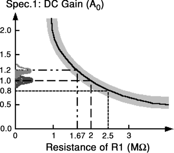
Fig. 4.
The relationship between specification A0
and parameter R1 becomes a band due to the processfluctuation.
The above probabilities can be obtained either di-
rectly from the relationship between the specification
and the parameter of the circuit or computed through
µ=µ ( p0 )
Monte Carlo simulation. In the previous low pass filter
σ=σ ( p0 )
circuit, if µ and ±3σ of R1 distribution are 2 (M�) and
±10% respectively, the probability curves, computedboth from equation derivation (solid line) and computersimulation (dotted line), of the circuit to pass specifica-
tion (0.8 ≤ A
0 ≤ 1.2) are shown in Fig. 6 with respect
to the value of R1.
In the above curves it can be seen that, when R
Fig. 5.
The distributions of a specification due to parame-
ter variations for the normal circuit ( p
equals to its nominal value (=2 M�) and all other
i = p0) and the faulty
circuit ( pi = K ). There is probability that the normal cir-cuit does not pass the specification due to the parameter
variations, and for the faulty circuit, there still also exists
Prob(R ---->A )
a small probability that the circuit pass the specification.
−(x−µ j (pi ))2
2σ 2( p
j (x , pi ) =
2πσ j ( pi )
where x is the value of specification s j located, µ j is
the mean value and σ 2 is the variance of specification
j . If there is a fault on pi , i.e., pi deviates to a new
value, K , s j will have a new distribution but with aform similar to that of Eq. (1). That the circuit passes
specification s j is sl ≤ s
j (x , pi ) ≤ suj
1.597 1.738
2.395 2.607
probability that the circuit passes s j when pi = K ,
(BF1) (BP1)
(BP2) (BF2)
represented as Prob( pi = K −→
pass sj), is:
Fig. 6.
Probability of the low pass circuit to pass specification
A0 with respect to the value of R1, where the nominal value is
� su −(x−µj(K))2
2.0 (M�). Bounds for parameter R1 to pass or fail A0 during
2σ 2(K )
i = K −→ s j =
testing for a 90% confidence level are shown. The central region
2πσ j (K ) slj
is the pass region, the two outside regions are fail regions, and the
two gray regions are uncertain regions.
Chang, Lee and Chen
parameters vary randomly within their respective ±3σ
around their nominal values, the filter always pass spec-
ification A
0, but will only "partially" pass A0 if R1 is
smaller than 1.8 (M�) or larger than 2.3 (M�). For
example, if R
1 = 2.4 (M�), the circuit has an approxi-
mate 90% probability to pass A0, and if R1 = 1.6 (M�),
it only has an approximate 10% probability to pass
this specification. If R1 is greater than 2.7 (M�) or
smaller than 1.5 (M�) the circuit will definitely fail
to pass A0.
The bounds of accepted and rejected range for pa-
rameters can be obtained by solving Eqs. (2) and (3)
under a given testing confidence (that is, after the test-
ing, even if the circuit passes all specification tests,
the circuit still has a certain probability of not work-
ing). For example, if the testing confidence is 90%, four
bounds solved for R
1 for A0 are shown in Fig. 6. They
are BF1 = 1.597 (M�), BP1 = 1.738 (M�), BP2 =
2.395 (M�) and BF2 = 2.607 (M�) respectively,where BF1 and BF2 are the lower and upper bound-
Fig. 7.
Elimination of specifications based on the locations of pass,
ary values respectively of the fail band, and BP1 and
fail, and uncertain regions between specifications for a parameter pk .
BP2 are lower and upper boundary values respectivelyof the pass region. The circuit will pass A0 (the DC gain
of rejected range for the i th parameter are:
specification) with over a 90% probability when R1 isbetween BP1 = 1.738 (M�) and BP2 = 2.395 (M�),
BF1i = maximum(BF1i1, BF1i2, . . , BF1in)
and will fail, with over a 90% probability, if R1 is be-
BF2i = minimum(BF2i1, BF2i2, . . , BF2in)
low BF1 = 1.597 (M�) or over BF2 = 2.607 (M�).
Within the two gray regions, i.e., BF1 = 1.597 (M�)
Hence, a specification Si can be neglected, for a pa-
and BP1 = 1.738 (M�), and BP2 = 2.395 (M�) and
rameter pk, when its bounds of pass range are outside
BF2 = 2.607 (M�), the circuit cannot be determined
bounds of another specification S j since a circuit which
to be "pass or fail" due to random variations, which are
passes S j will always pass Si as shown in Fig. 7(a). For
caused by the process fluctuation, of other parameters.
the case in Fig. 7(b), S j can be ignored because it is
If we reduce the testing confidence, these two regions
"dominated" by Si for pk lower bound fault and, on the
will shrink. For example, if we only ask for a testing
other hand, "dominated" by Sk for pk upper bound fault.
confidence of 50%, these two regions will shrink to
However, for the case of Fig. 7(c), neither S j nor Sk can
zero and the problems of setting the fault boundaries,
be neglected since there are overlap between their re-
consequently the specification reduction, will be sim-
spective gray regions. When the parameter value, for
plified to that as stated previously in Section 2.
example, pkf , falls into these gray regions, there is al-
For the general i th parameter ( p
ways a probability that the CUT will not pass either of
i ) for the j th speci-
fication, we denote the above four bounds to be BP1
the specifications.
Hence, for the testing purpose, we can define
i j , BF1i j , and BF2i j respectively. If a circuit is
fault-free, it should satisfy "all" specifications, and the
"redundancy" for specifications as following:
bounds of the accepted range for the i th parameter aregiven by:
(a) A specification S
j is "lower bound redundant" for
i = maximum(BP1i1, BP1i2, . . , BP1in)
a parameter pk, if a specification Si,i�= j exists such
BP2i = minimum(BP2i1, BPi2, . . , BP2in)
that BF1ki ≥ BP1kj .
(b) A specification S j is "upper bound redundant" for
On the other hand, a circuit is considered to be faulty
a parameter pk, if a specification Si,i�= j exists such
if it violates one of specifications. Hence, the bounds
that BP2kj ≥ BF2ki .
Structural Fault Based Specification Reduction
filter circuit [6], as shown in Fig. 9(a), is used to demon-strate the procedure, as well as its efficiency.
For this circuit, the band-pass output (BPO) is taken
as the output and R1 = R2 = R3 = R4 = R6 = 1 M,C1 = C2 = 200 p, R6 = 300 K, and R7 = 700 K.
The central frequency for the band-pass output (BPO),
fc = (2π R3C1R4C2)−1 = 795 Hz with a gain
Fig. 8.
(a) The 2-dimensional probability bell for passing specifica-
equal to 1.11. The frequency response of the circuit is
tion S j test for the double-parameters ( pm , pn) fault; (b) The circlet,
shown in Fig. 9(b). The operational amplifiers in this
which is cut from the 2-dimensional cone of (a) for a test confidence
circuit are the benchmark operational amplifier [6], as
shown in Fig. 10. It is adopted for the purpose to makethe study more practical. The technology file used for
(c) A specification is "redundant" for testing, i.e., it can
all computer simulation in the study is TSMC CMOS
be removed, if it is both lower bound redundant and
0.8 um SPDM technology file of under a ±2.5 V supply
upper bound redundant for all parameters.
voltage. The specifications of the filter are shown inTable 3.
In above, we presented the approach of specification
With the fault model described previously, the num-
reduction based on soft (parametric) faults. However,
ber of parameters (R, C, and W /L and VT of each tran-
the above approach also applies to hard faults since
sistor) is 66. To study the effects on specifications of
when a hard fault occurs, the circuit often fails at least
all the faults of parameters, a Monte Carlo simulation
one specification.
by considering a 10% (=3σ ) variation on parameter
In the above, in order to obtain the probability curves,
values has been performed. Table 4 summarizes the
Monte Carlo simulation needs to be done, which is
simulated results where the mean and variance of each
a time consuming process. Time complexity may be
specification are listed. The results are in two groups:
a problem large size circuits are considered. One ap-
one group is for parameters in operational amplifiers,
proach to alleviate this difficulty is to partition the CUT
and the other group is for passive component param-
into several small blocks and the simulation is done
eters outside operational amplifiers. In the table, the
hierarchically [3].
variance of each specification caused by the parame-
Also, in the above, we deal with only single parame-
ters inside operational amplifiers is much smaller than
ter fault [5, 13]. When more than two parameter faults
that caused by the passive components outside oper-
are considered, the case will be more complex. To ex-
ational amplifiers. This is obvious since devices and
plain, for simplicity, a double fault ( p
components in an operational amplifier are insensitive
m , pn ) case is
used as an example. When a double parameters fault is
to the characteristics of the operational amplifier due to
considered, the probability curve for one specification,
negative feedback. Hence, in the forgoing study, only
the passive components (R1–R7, C1, C2) outside op-
i , will become a three-dimensional cone as shown
in Fig. 8(a) rather than the two-dimensional curve of
erational amplifiers are considered.
Fig. 6. For a given confidence level, a circlet will be
Table 5 shows the bounds (BF1, BP1, BP2, BF2) ob-
cut on the cone as shown in Fig. 8(b). Similarly, when
tained from simulations for all specifications w.r.t. C1
another specification, saying S
under 99%, 90% and 50% testing confidence. From the
j is also considered for
reduction, another circlet can also be obtained. If the
table, it is seen that C1 is insensitive to specifications
circlet of S
1 and 7 because, even if a large deviation occurs in C1,
j covers the circlet of Si , then S j is domi-
nated by S
the circuit always passes testing for these specifica-
i for this double ( pm , pn ) fault. As a result, S j
can be neglected when testing for the double-parameter
tions. Also, decreasing the testing confidence reduces
the uncertain ranges (BF1–BP1 and BP2–BF2) and a50% testing confidence gives a zero uncertain range.
The essential lower bound specification (ELBS) and
essential upper bound specification (EUBS) for C1 arealso derived. For the 99% testing confidence case, the
To further illustrate the above specification reduction
maximum{BF1's} is 154 (pF) from specification S2
approach, a benchmark continuous-time state-variable
(this means that if a defect causes C2 smaller than 154
Chang, Lee and Chen
Fig. 9.
(a) The circuit of the benchmark continuous-time state-variable filter. (b) Frequency
response of band-pass output.
(pF), there is a 99% probability that the circuit will
decrease fault. Hence, the ELBS's are S2, S4, S5 and
fail the test). However, for S1, S3, S6, S7, S9 and S10,
S8. On the other hand, the EUBS's are S2, S4, S5, S6
their BP1 values are all smaller than 154 (pF), i.e., these
and S9 because their BF2 values are smaller than the
specifications can be ignored when considering the C1
minimum{BF2's} = 260 (pF), which is derived from
Table 3.
Specifications of the filter circuit and their
nominal values (NV), lower bounds (LB), and upperbounds (UB).
S1: Gain @ fc
S2: Central frequency ( fc)
S3: Low cutoff frequency
S4: High cutoff frequency
S5: 3 dB bandwidth
S6: Quality factor
S7: Gain @ 100 Hz
S8: Gain @ 700 Hz
S9: Gain @ 900 Hz
Fig. 10.
Schematic representation and element values of benchmark
S10: Gain @ 10 KHz
CMOS operational amplifier.
Structural Fault Based Specification Reduction
Table 4.
Means and variances of specifications caused by variations of device parameters inside operational amplifiers and
by passive component parameters outside operational amplifiers.
Caused by the variations of device
Caused by the variations of passive
parameters in opamps
R and C outside opamps
S1: Gain @ fc
S2: Central frequency ( fc)
S3: Low cutoff frequency
S4: High cutoff frequency
S5: 3 dB bandwidth
S6: Quality factor
S7: Gain @ 100 Hz
S8: Gain @ 700 Hz
S9: Gain @ 900 Hz
S10: Gain @ 10 KHz
Table 5.
Bounds of pass and fail range for all specifications w.r.t. C1 under 99%, 90% and 50% testing
confidence (unit: pF) (∞ : infinity).
S2 also. Combining ELBS's and EUBS's, we obtain the
some specifications can be ignored. Also, as the testing
essential test specifications (ETS) for the C1 deviation
confidence is decreased, the number of ignored speci-
fault are S2, S4, S5, S6, S8 and S9.
In a similar way, the ETS's for all component pa-
To study the effect of hard faults, a total of 36 short
rameters can be obtained. The final reduced test spec-
(bridging) faults between nine circuit nodes (4 internal
ification set is a set of the union of the ETS's of all
nodes, HPO, BPO, LPO, input and ground) are sim-
component parameters. Table 6 shows the ETS's for
ulated. For a short fault, a short resistance of 10 (�)
all component parameters, the final reduced test speci-
is assumed. Table 7 lists the number of short faults
fications and the ignored test specifications under 99%,
detected when all the above specifications are consid-
90% and 50% testing confidence, respectively. It can
ered. All of 36 short faults can be detected. Even for S1
be seen that in general certain number of test speci-
testing, it can detect 33 faults and for S2 testing, it can
fications can be reduced for a component parameter
detect 32 faults. With S1 and S2 testing simultaneously,
and when all parameters are considered, there are still
all 36 short faults are detected. This demonstrates that
Chang, Lee and Chen
Table 6.
Essential test specifications for each component parameter under 99%, 90% and 50% testing
Final test specs.
Ignored test specs.
Table 7.
Number of detected hard faults for each specification.
the specification test can easily detect hard faults. If a
hard fault can not be detected by all specification test,this fault can be effectively considered as a redundant
We acknowledge the many discussions we had on the
fault since it does not affect the performance of the
subject of this paper with Prof. C.C. Su of the National
Central University, Taiwan.
1. B. Atzema and T. Zwemstra, "Exploit Analog IFA to Improve
In this paper, we have presented an approach to reduce
Specification Based Tests [of SC Circuits]," in Proceedings of
the number of test specifications for analog circuits.
European Design and Test Conference, 1996, pp. 542–546.
The approach starts with derivation of the relationship
2. R.R. Boyd, Tolerance Analysis of Electronic Circuit Using Math-
between specifications and device and/or component
cad, CRC Press, 2000.
3. E. Felt, S. Zanella, C. Guardiani, and A.L. Sangiovanni-
parameters then defines upper and lower bounds for
Vincentelli, "Hierarchical Statistical Characterization of Mixed-
parameters to find essential test specifications. Then
Signal Circuits Using Behavioral Modeling," in Proc. IEEE In-
the variations on component parameters due to fab-
ternational Conference on Computer-Aided-Design, San Jose,
rication process fluctuations are considered by using
CA, November 1996.
a statistical model to reduce test specifications with a
4. S.D. Huss, R.S. Gyurcsik, and J.J. Paulos, "Optimal Ordering of
Analog Integrated Circuit Tests to Minimize Test Time," in Pro-
testing confidence probability. A continuous time state-
ceedings of Design Automation Conference, 1991, pp. 494–499.
variable filter example circuit has been used to demon-
5. S.D. Huynh, K. Seongwon, M. Soma, and J. Zhang, "Automatic
strate the specification reduction procedure and it has
Analog Test Signal Generation Using Multifrequency Analysis,"
been shown that 2, 3 or 4 out of 10 specifications can
IEEE Transactions on Circuits and Systems II: Analog and Dig-
be ignored during specification testing under the 99%,
ital Signal Processing, vol. 46, no. 5, pp. 565–576, May 1999.
6. B. Kaminska, K. Arabi, I. Bell, P. Goteti, J.L. Huertas, B. Kim,
90% and 50% testing confidence level respectively. The
A. Rueda, and M. Soma, "Analog and Mixed-Signal Benchmark
procedure is effective and can be used in manufacturing
Circuits—First Release," in Proceeding of International Test
specification test for analog circuits to reduce test time.
Conference, 1997, pp. 183–190.
Structural Fault Based Specification Reduction
7. W.M. Lindermeir, H.E. Graeb, and K.J. Antreich, "Analog
18. D.M.H. Walker, Yield Simulation for Integrated Circuits,
Testing by Characteristic Observation Inference," IEEE Trans-
Boston, MA: Kluwer Academic Publishers, 1987.
actions on Computer-Aided Design of Circuits and Systems,vol. 18, no. 9, pp. 1353–1368, September 1999.
8. A. Meixner and W. Maly, "Fault Modeling for the Testing
Soon-Jyh Chang was born in Taiwan 1969. He received his M.S.
of Mixed Integrated Circuits," in Proc. International Test
degree in Electronic Engineering from National Chiao-Tung Univer-
Conference, 1991, pp. 564–572.
sity, Hsin-Chu, Taiwan, in 1996. He is currently working towards
9. L. Milor and A.L. Sangiovanni-Vincentelli, "Minimizing
his Ph.D. degree at NCTU. His research interests including test
Production Test Time to Detect Faults in Analog Integrated
generation and design for testability for analog and mixed-signal
Circuits," IEEE Transactions on Computer-Aided Design,
vol. 13, no. 6, pp. 796–813, June 1994.
10. C.Y. Pan and K.T. Cheng, "Pseudorandom Testing for Mixed-
Chung-Len Lee received BS degree in electrical engineering from
Signal Circuits," IEEE Transaction on Computer-Aided Design
National Taiwan University, Taiwan, R.O.C., in 1968. He obtained his
of Integrated Circuits and Systems, vol. 16, pp. 1173–1185,
M.S. and Ph.D. Degree in Electrical Engineering, Carnegie-Mellon
October 1997.
University, U.S.A., in 1971 and 1975 respectively. From 1975, he
11. M. Sachdev and B. Atzema, "Industrial Relevance of Analog
has been a professor of Electronic Engineering at National Chiao-
IFA: A Fact or a Fiction," in Proceeding of International Test
Tung University in Taiwan, and was the director of Semiconductor
Conference, 1995, pp. 61–70.
Research Center of the university in the period of 1980–1983. From
12. S. Sen, S.S. Nath, V.N. Malepati, and K.R. Pattipati,
1989 to present, he is the director of the Training Center for Sub-
"Simulation-Based Testability Analysis and Fault Diagnosis," in
micron Professionals of the university and supervised more than
Conference Record of Test Technology and Commercialization,
100 M.S. and Ph.D. students to complete their thesis work that result
1996, pp. 136–148.
in more than 200 journal and conference papers published. His re-
13. M. Slamani and B. Kaminska, "Multifrequency Analysis of
search interests are in the area of semiconductor processes, material
Faults in Analog Circuits," IEEE Design & Test of Computers,
and devices, integrated circuit design, VLSI testing, and integrated
vol. 12, no. 2, pp. 70–80, Summer 1995.
optics. He has been involved in various technical activities in the
14. M. Soma, "An Experimental Approach to Analog Fault Mod-
above areas in Taiwan as well as in Asia. He is a senior member of
els," in Proceeding of Custom Integrated Circuits Conference,
IEEE and member of editorial board, Journal of Electronic Testing:
1991, pp. 13.6/1–13.6/4.
Theory, and Application.
15. T.M. Souders and G.N. Stenbakken, "Cutting the High Cost of
Testing," IEEE Spectrum, March 1991, pp. 48–51.
16. S. Sunter and N. Nagi, "Test Metrics for Analog Parame-
Jwu E. Chen received BS, MS, and Ph.D. degrees in electronic en-
tric Faults," in Proceeding of VLSI Test Symposium, 1999,
gineering from National Chiao-Tung University, Taiwan, in 1984,
pp. 226–234.
1986 and 1990 respectively. Presently, he is an sssociate professor
17. R. Voorakaranam and A. Chatterjee, "Test Generation for
of Electrical Engineering of Chung-Hua University, Taiwan. His re-
Accurate Prediction of Analog Specifications," in Proceeding
search interests are in reliability, fault tolerant and test quality of
of VLSI Test Symposium, 2000, pp. 137–142.
Source: http://sscas.ee.ncku.edu.tw/web/files/journal/2002JETTA_Structural_Fault_Based_Specification_Reduction_for_Testing_Analog_Circuits.pdf
MSDS#: KIP070102-PPC Material Safety Data Sheet Page 1 of 1 CRYSTAL NAILS MASTER POWDER CLEAR Section 1 – Identification of the Substance/Preparation and of the Company/Undertakin Material/Product Name: Master Powder Clear MSDS Initial Approval Date: Chemical Name: N/A MSDS Prepared by: BSQ
WWP – Work with Perpetrators of Domestic Violence in Europe – Daphne II Project 2006 - 2008 Directrices para el desarrollo de unas normas para los programas dirigidos a los hombres perpetradores de la violencia doméstica Version 1.1 Introducción La violencia ejercida contra las mujeres ocurre en todos los países de Europa, siendo un problema serio y generalizado. Este tipo de violencia es una manifestación de la desigualdad en las relaciones de poder entre los hombres y las mujeres, que ha llevado a la dominación sobre y discriminación contra las mujeres por parte de los primeros, al impedimento de su desarrollo íntegro, representando una violación omnipresente de los derechos humanos y obstáculo importante a la igualdad de género1. Los estados miembros de los organismos internacionales, como las NN.UU. y el Consejo Europeo, y también los países de la UE, están vinculados por leyes internacionales y nacionales a ejercitar la diligencia debida para prevenir, investigar y castigar los actos de violencia, sean perpetrados por el estado o por personas físicas, y de proveer de ayuda a las víctimas2. La violencia doméstica contra las mujeres supone un patrón de comportamiento controlador por parte de la (ex) pareja íntima, que incluye, sin ser excluyente, la violencia física y sexual, el maltrato emocional, el aislamiento, la violencia económica, las amenazas, la intimidación, y el acoso3. La violencia contra las mujeres en la familia también afecta a sus hijos/as, que, a su vez, tienen el derecho a ser protegidos y recibir apoyo.